D21m System
6-28 D21m Modules Date printed: 30.08.07
S1.4
S1.4 PCM Latency (Module 2 only)
OFF
PCM signal is delayed by 1 video frame (factory default)
ON
PCM signal is minimally delayed
Same as S2.4 above, but for module 2.
S1.5
S1.5 Module 2 Pulldown Mode
OFF
Pulldown mode is off (factory default)
ON
Pulldown mode is on
Same as S2.5 above, but for module 2.
S1.6
S1.6 Module 2 Con guration Download
OFF
Standard operation (factory default)
ON
Con guration download via RS232
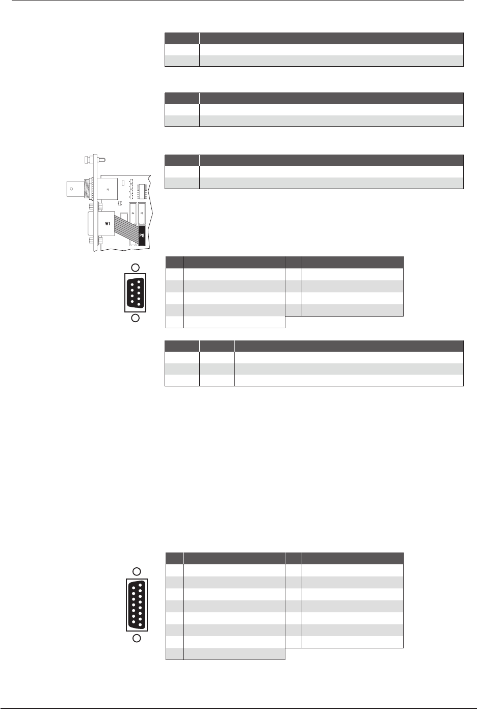
If rmware download to decoder module 2 is required, plug the short at
cable (W1) coming from the METADATA OUT front-panel socket to the
PCB socket P8 (labeled UPDATE2).
The pin assignment of the METADATA OUT socket (9-pin D-type, female)
in this case is as follows:
Pin Signal Pin Signal
1
n.c.
6
n.c.
2
DOUT_2
7
n.c.
3
DIN_2
8
n.c.
4
n.c.
9
n.c.
5
n.c.
S1.7 / S1.8
S1.7 S1.8 Downmix to Ch 7/8 (or 15/16, resp.)
OFF OFF
No downmix (factory default)
ON OFF
Automatic downmix
OFF ON
Forced downmix
Metadata and Downmixing: A Dolby
®
E stream contains metadata with
various information on the encoded signal. This information can be read
out from the front panel connector. The Vi Dolby
®
E decoder card only
uses this information in case a 2-channel stereo downmix is required from
a 5.1-channel surround signal within the Dolby
®
E stream; then the decoder
interprets the center and surround channel levels and uses them for the internal
downmixer that is activated by the DIP switches S1.7 and S1.8. The downmix
can be made constantly available and, subsequently, overwriting any audio
data that was contained on these channels beforehand (“forced downmix”), or
it is possible to “ ll” the channels 7/8 or 15/16 only if the metadata indicate
that these channels are not being used otherwise (automatic downmix).
Connector Pin Assignments: 2 x AES IN MAIN/PCM (15-pin D-type, female)
Pin Signal Pin Signal
1
Main In 1 +
9
Main In 1 –
2
Main In 1 Chassis
10
PCM Delay In 1 Chassis
3
PCM Delay In 1 –
11
PCM Delay In 1 +
4
n.c.
12
n.c.
5
Main In 2 +
13
Main In 2 –
6
Main In 2 Chassis
14
PCM Delay In 2 Chassis
7
PCM Delay In 2 –
15
PCM Delay In 2 +
8
n.c.
1
8
15
9
Solder/Crimp View
(or Socket View)
1
5
9
6
Solder/Crimp View
(or Socket View)

