16
Explanation for circuit operation
The detailed specifications of this IC are as follows.
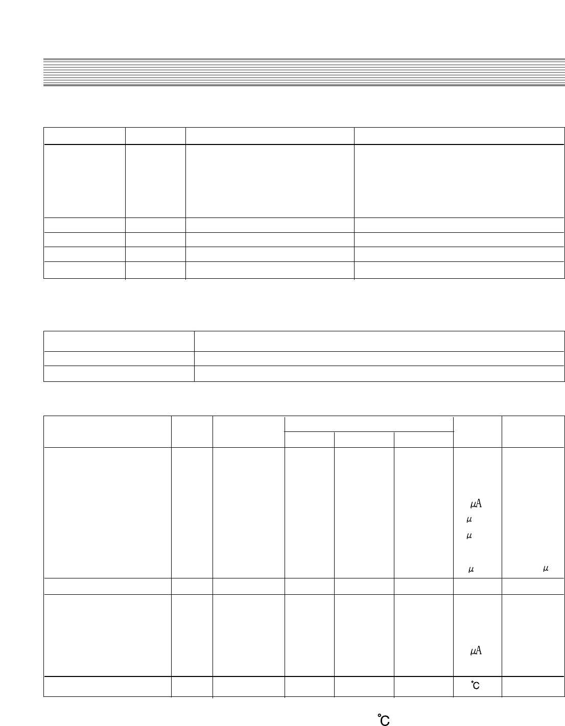
Terminal No. Symbol Name Functions
1O.
Overcurrent/Feedback terminal Overcurrent detection signal
C.
P. /
F.
B
2S
Source terminal MSOFET source
3 D Drain terminal MOSFET drain
4 Vin Power terminal Control circuit power input
5 GND Ground terminal Ground
<Functions of each terminal>
Symbol Functions
O.V.P Overvoltage protection circuit built-in
T.S.D Overheat protection circuit built-in
<Other functions>
Specifications
Item Terminal Symbol
MAX TYP MAX
Unit
Operation start power voltage
4 - 5 VIN(ON) 14.4 16 17.6 V
Operation stop power voltage
4 - 5 VIN(OFF) 9 10 11 V
Circuit current at operation 4 - 5 IIN(ON) - - 30 mA
Circuit current at non-operation
4 - 5 IIN(OFF) - - 100 -
Maximum OFF time - TOFF(MAX) 45 - 55
Minimum Quasi-Resonance 1 - 5 Tth(2) - - 1.0
signal input time
Minimum OFF time - TOFF(MIN) - - 1.5
OOP/FB terminal threshold voltage
1 - 5 Vth(1) 0.68 0.73 0.78 V -
OOP/FB terminal threshold voltage 2
1 - 5 Vth(2) 1.3 1.45 1.6 V
OOP/FB terminal outflow current
1 - 5 IOCP/FB 1.2 1.35 1.5 mA
OVP operating power voltage
4 - 5 VIN(OVP) 20.5 22.5 24.5 V -
Latch circuit sustaining current
4 - 5 IIN (H) - - 400
Latch circuit clearing power voltage
4 - 5 VIN(LA.OFF) 6.6 - 8.4 V
Overheat protection temp.
- Tj(TSD) 140 - -
< Electrical features of control area:(Ta=25 ), Vin=18V >

